- 您现在的位置:买卖IC网 > Sheet目录492 > NTQS6463R2 (ON Semiconductor)MOSFET P-CH 20V 6.8A 8-TSSOP
�� �
�
�NTQS6463�
�Power� MOSFET�
�?20� V,� ?6.8� A,� P?Channel� TSSOP?8�
�Features�
�?� New� Low� Profile� TSSOP?8� Package�
�?� Ultra� Low� R� DS(on)�
�?� Higher� Efficiency� Extending� Battery� Life�
�?� Logic� Level� Gate� Drive�
�?� Diode� Exhibits� High� Speed,� Soft� Recovery�
�?� Avalanche� Energy� Specified�
�?� I� DSS� and� V� DS(on)� Specified� at� Elevated� Temperatures�
�Applications�
�?� Power� Management� in� Portable� and� Battery?Powered� Products,� i.e.:�
�Computers,� Printers,� PCMCIA� Cards,� Cellular� and� Cordless�
�Telephones�
�?�
�Lithium� Ion� Battery� Applications�
�?�
�Note� Book� PC�
�MAXIMUM� RATINGS� (T� C� =� 25� °� C� unless� otherwise� noted)�
�V� DSS�
�?20� V�
�G�
�http://onsemi.com�
�R� DS(on)� TYP�
�20� m� W� @� ?10� V�
�P?Channel�
�D�
�I� D� MAX�
�?6.8� A�
�Rating�
�Drain?to?Source� Voltage�
�Gate?to?Source� Voltage�
�Symbol�
�V� DSS�
�V� GS�
�Value�
�?20�
�"� 12�
�Unit�
�V�
�V�
�S�
�MARKING�
�Drain� Current� (Note� 1)�
�?� Continuous� @� T� A� =� 25� °� C�
�?� Continuous� @� T� A� =� 70� °� C�
�?� Pulsed� (Note� 3)�
�Total� Power� Dissipation� (Note� 1)�
�@� T� A� =� 25� °� C�
�I� D�
�I� D�
�I� DM�
�P� D�
�?5.5�
�?4.4�
�"� 30�
�0.93�
�A�
�W�
�8�
�1�
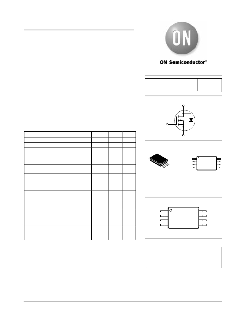
�TSSOP?8�
�CASE� 948S�
�PLASTIC�
�DIAGRAM�
�463�
�YWW�
�N�
�Drain� Current� (Note� 2)�
�?� Continuous� @� T� A� =� 25� °� C�
�?� Continuous� @� T� A� =� 70� °� C�
�?� Pulsed� (Note� 3)�
�Total� Power� Dissipation� (Note� 2)�
�@� T� A� =� 25� °� C�
�I� D�
�I� D�
�I� DM�
�P� D�
�?6.8�
�?5.4�
�"� 30�
�1.39�
�A�
�W�
�463�
�Y�
�WW�
�N�
�=� Device� Code�
�=� Year�
�=� Work� Week�
�=� MOSFET�
�Operating� and� Storage�
�T� J� ,� T� stg�
�?55� to�
�°� C�
�PIN� ASSIGNMENT�
�Temperature� Range�
�+150�
�Single� Pulse� Drain?to?Source� Avalanche�
�Energy� ?� Starting� T� J� =� 25� °� C�
�(V� DD� =� 40� V,� I� L� =� 18.4� A,�
�L� =� 5.0� mH,� R� G� =� 25� W� )�
�Thermal� Resistance� ?�
�E� AS�
�R� q� JA�
�845�
�mJ�
�°� C/W�
�D�
�S�
�S�
�G�
�2�
�3�
�4�
�1�
�8�
�7�
�6�
�5�
�D�
�S�
�S�
�D�
�Junction?to?Ambient� (Note� 1)�
�Junction?to?Ambient� (Note� 2)�
�134�
�90�
�Top� View�
�Maximum� ratings� are� those� values� beyond� which� device� damage� can� occur.�
�Maximum� ratings� applied� to� the� device� are� individual� stress� limit� values� (not�
�ORDERING� INFORMATION�
�normal� operating� conditions)� and� are� not� valid� simultaneously.� If� these� limits� are�
�exceeded,� device� functional� operation� is� not� implied,� damage� may� occur� and�
�reliability� may� be� affected.�
�1.� Minimum� 3� ″� X� 3� ″� FR?4� board,� steady� state.�
�2.� Mounted� on� 1� ″� square� (1� oz.)� board,� steady� state.�
�3.� Pulse� Test:� Pulse� Width� =� 300� m� s,� Duty� Cycle� =� 2%.�
�Device�
�NTQS6463�
�NTQS6463R2�
�Package�
�TSSOP?8�
�TSSOP?8�
�Shipping� ?�
�100� Units/Rail�
�3000/Tape� &� Reel�
�?For� information� on� tape� and� reel� specifications,�
�including� part� orientation� and� tape� sizes,� please�
�refer� to� our� Tape� and� Reel� Packaging� Specification�
�Brochure,� BRD8011/D.�
�?� Semiconductor� Components� Industries,� LLC,� 2004�
�September,� 2004� ?� Rev.� 2�
�1�
�Publication� Order� Number:�
�NTQS6463/D�
�发布紧急采购,3分钟左右您将得到回复。
相关PDF资料
NTR0202PLT1
MOSFET P-CH 20V 400MA SOT-23
NTR1P02LT3G
MOSFET P-CH 20V 1.3A SOT23-3
NTR1P02T1
MOSFET P-CH 20V 1A SOT-23
NTR2101PT1G
MOSFET P-CH 8V 3.7A SOT-23
NTR3161NT1G
MOSFET N-CH 20V 3.3A SOT-23
NTR3162PT3G
MOSFET P-CH 20V 2.2A SOT-23
NTR4003NT1G
MOSFET N-CH 30V 500MA SOT-23
NTR4101PT1G
MOSFET P-CH 20V 1.8A SOT-23
相关代理商/技术参数
NTQS6466
制造商:未知厂家 制造商全称:未知厂家 功能描述:TRANSISTOR | MOSFET | N-CHANNEL | 20V V(BR)DSS | 6.8A I(D) | SO
NTQS6466/D
制造商:未知厂家 制造商全称:未知厂家 功能描述:Power MOSFET 6.8 Amps, 20 Volts
NTR0202PL
制造商:ONSEMI 制造商全称:ON Semiconductor 功能描述:Power MOSFET −20 V, −400 mA, P−Channel SOT−23 Package
NTR0202PL/D
制造商:未知厂家 制造商全称:未知厂家 功能描述:Power MOSFET 400 mA 20 V P-Channel SOT-23
NTR0202PL_06
制造商:ONSEMI 制造商全称:ON Semiconductor 功能描述:Power MOSFET -20 V, -400 mA, P-Channel SOT-23 Package
NTR0202PLT1
功能描述:MOSFET -20V -400mA RoHS:否 制造商:STMicroelectronics 晶体管极性:N-Channel 汲极/源极击穿电压:650 V 闸/源击穿电压:25 V 漏极连续电流:130 A 电阻汲极/源极 RDS(导通):0.014 Ohms 配置:Single 最大工作温度: 安装风格:Through Hole 封装 / 箱体:Max247 封装:Tube
NTR0202PLT1G
功能描述:MOSFET -20V -400mA P-Channel RoHS:否 制造商:STMicroelectronics 晶体管极性:N-Channel 汲极/源极击穿电压:650 V 闸/源击穿电压:25 V 漏极连续电流:130 A 电阻汲极/源极 RDS(导通):0.014 Ohms 配置:Single 最大工作温度: 安装风格:Through Hole 封装 / 箱体:Max247 封装:Tube
NTR0202PLT1G-CUT TAPE
制造商:ON 功能描述:NTR Series P-Channel 20 V 550 mOhm 225 mW Surface Mount Power MOSFET - SOT-23